
Wafer bonding - Adhesive Bonding
Wafer bonding, or chip and wafer bonding, typically refers to a technology that utilizes different physical or chemical mechanisms to combine two or more wafers (homogeneous/heterogeneous) to achieve mutual integration of different materials or functional layers, in order to enhance the performance and reliability of devices, resulting in the formation of reactive covalent bonds, metallic bonds, etc. at the interface. It is used for heterojunction bonding, eutectic bonding, anodic bonding, adhesive bonding, etc., and is widely applied in fields such as CIS, MEMS, NAND, DRAM, advanced logic, and advanced packaging.
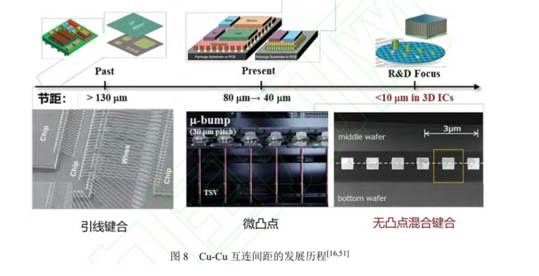
There are many ways of bonding. In the early days, chips were connected through gold or copper wires.
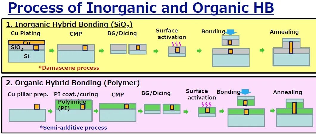
The polyimide (PI) materials used in wafer bonding mainly include the following types and characteristics:
Ordinary polyimide (PI)
Characteristics: High temperature resistance (long-term use temperature 200-400℃), chemical corrosion resistance, high mechanical strength, can be used as an intermediate layer to achieve wafer bonding, and can achieve PI-PI bonding or hetero-bonding with other materials (such as PDMS) by adjusting the curing cycle. Applications: Suitable for low temperature bonding (temperature<300℃), commonly used in flexible MEMS, three-dimensional integration, and other scenarios, capable of filling micron-level undulations on the wafer surface without requiring additional planarization treatment.
Photosensitive polyimide (PSPI)
Characteristics: By introducing photosensitive groups, patterning can be achieved through the "coating-exposure-development-curing" process, with precision reaching the nanometer level. It combines the high temperature resistance and insulating properties of PI. Applications: Used for wafer bonding in high-density interconnection, especially in advanced packaging such as AI chips and HBM (High Bandwidth Memory), it can precisely define the bonding area and reduce alignment errors.
High heat-resistant resin polyimide
Characteristics: Higher elastic modulus, superior control of total wafer thickness deviation (≤1.0μm), free of regulated harmful components (such as NMP, PFAS), and resistance to high-temperature processes above 300℃. Applications: Specifically designed for bonding ultra-thin wafers (thickness ≤50μm), suitable for advanced processes such as power devices, 3D ICs, and TSVs (Through-Silicon Vias), effectively addressing issues of deformation and uneven pressure during wafer thinning.
Nanocomposite polyimide
Characteristics: By incorporating nanoparticles (such as boron nitride nanotubes, silicon dioxide, etc.), it enhances thermal conductivity, reduces dielectric constant, and combines mechanical strength with thermal dissipation performance. Applications: It is suitable for high-performance computing chips and heterogeneous integration scenarios, reducing signal delay and enhancing thermal management efficiency at the bonding interface.
The selection of these PI materials must be tailored to specific process requirements (such as bonding temperature, wafer thickness, interconnect density, etc.) and performance criteria (such as heat resistance, insulation, mechanical strength) to achieve reliable wafer bonding.
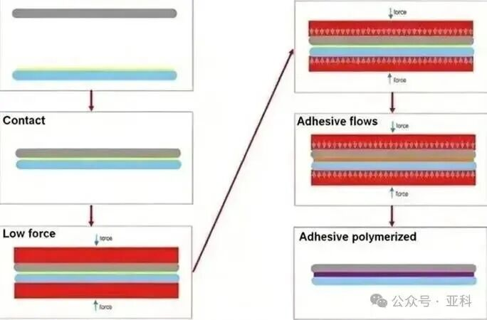
Use intermediate polymer layers (such as BCB, polyimide, photoresist) as adhesives. Form a polymer film on the wafer through methods such as spin coating, and then bond the two wafers together at a relatively low temperature (usually<400°C) and pressure.
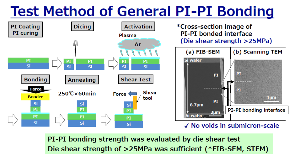
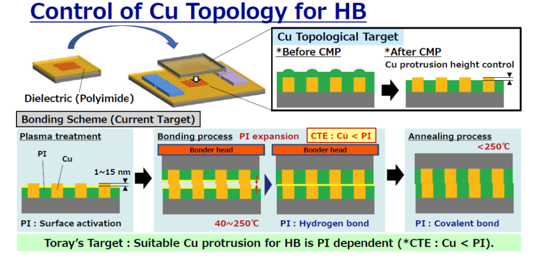
Polymer bonding, as one of the key technologies for chip stacking in three-dimensional integrated circuits, relies on the adhesion and cohesion properties of polymer materials to establish mechanical connections. Its process characteristics and material selection profoundly affect the performance and reliability of integrated systems. The core advantage of this technology lies in its low-temperature (typically<200°C) and low-pressure (typically <1 MPa) process conditions, which significantly reduce thermal stress damage to molded devices and are highly compatible with CMOS processes. Additionally, the polymer layer can effectively fill micron-scale undulations (roughness
The current mainstream polymer bonding materials focus on thermosetting resin systems. Among them, benzocyclobutene (BCB) and polyimide (PI) dominate due to their excellent thermal stability (glass transition temperature >350°C), low moisture absorption (
Alignment error control is a core challenge in polymer bonding, with sources including initial deviations before bonding, thermal expansion differences induced by CTE mismatch between upper and lower layers (<2ppm/℃), and interlayer slippage caused by polymer softening during the bonding process (5-10μm). To mitigate the slippage effect, the industry is exploring nanoscale surface texturing techniques to enhance interlayer friction through increased mechanical interlocking. Meanwhile, hybrid bonding schemes (such as polymer-metal composite bonding) introduce metal bumps locally to improve alignment accuracy in critical areas (<500nm) while maintaining overall flexibility. Recent research also focuses on the development of high thermal conductivity polymer materials, such as composite resins filled with boron nitride nanotubes, whose thermal conductivity has exceeded 2W/m·K, representing a 300% improvement over traditional materials.
mail:wuping@csc-ic.com ; angel@csc-ic.com

right 2023. Chinaic Technology Co. ,Ltd. All Rights Reserved 粤ICP备13001812号
