Uncover the whole process of semiconductor manufacturing (Part 2)
In this issue, we will continue to explore two key steps in semiconductor manufacturing: etching and thin film deposition.
Step 4: etching
After the lithography of the circuit diagram is completed on the wafer, the etching process is used to remove any excess oxide film and leave only the semiconductor circuit diagram. To do this, you need to use liquid, gas or plasma to remove the selected excess.
There are two main etching methods, depending on the materials used: wet etching using specific chemical solution for chemical reaction to remove oxide film, and dry etching using gas or plasma.
Wet etching
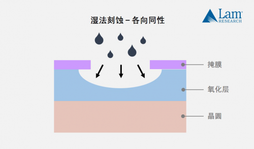
Wet etching using chemical solution to remove oxide film has the advantages of low cost, fast etching speed and high productivity. However, wet etching has the characteristics of isotropy, that is, its velocity is the same in any direction. This will lead to the mask (or sensitive film) and the etched oxide film can not be fully aligned, so it is difficult to deal with very fine circuit diagrams.
Dry etching
Dry etching can be divided into three different types. The first is chemical etching, which uses etching gas (mainly hydrogen fluoride). Like wet etching, this method is isotropic, which means it is not suitable for fine etching.
The second method is physical sputtering, that is, the ions in the plasma are used to impact and remove the excess oxide layer. As an anisotropic etching method, sputtering etching has different etching speeds in horizontal and vertical directions, so its fineness is also higher than chemical etching. However, the disadvantage of this method is that the etching speed is slow, because it completely depends on the physical reaction caused by ion collision.
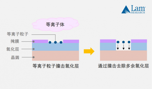
The final third method is reactive ion etching (RIE). RIE combines the first two methods, that is, while ionizing physical etching with plasma, chemical etching with the help of free radicals generated after plasma activation. In addition to the higher etching speed than the first two methods, RIE can use the characteristics of ion anisotropy to realize the etching of high-precision patterns.
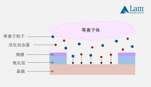
Nowadays, dry etching has been widely used to improve the yield of fine semiconductor circuits. It is very important to maintain the uniformity of full wafer etching and improve the etching speed. Today's most advanced dry etching equipment is supporting the production of the most advanced logic and memory chips with higher performance.
For different etching applications, Fanlin group provides a number of etching product lines, including dsie for deep silicon etching ™ Series and syndion ® Flex series, key dielectric etching products ® Series, Kiyo for conductor etching ® Series, versys for metal etching ® Metal series. Based on the industry-leading Kiyo and flex process modules, Fanlin group also launched sense. I in March last year ® Series, its high performance can meet the accuracy and consistency requirements required by the above production process, and is suitable for various key and semi critical etching applications.
Step 5: thin film deposition
In order to create micro devices inside the chip, we need to continuously deposit layers of thin films and remove the excess parts by etching. In addition, we need to add some materials to separate different devices. Each transistor or memory cell is built step by step through the above process. By "thin film" we mean that the thickness is less than 1 micron( μ m. Millionths of a meter), which cannot be manufactured by ordinary machining methods. The process of placing a thin film containing the required molecular or atomic units on a wafer is "deposition".
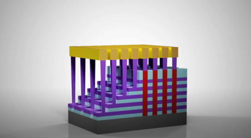
To form a multi-layer semiconductor structure, we need to first manufacture device laminations, that is, alternately stack multi-layer thin metal (conductive) films and dielectric (insulating) films on the wafer surface, and then remove the excess parts and form a three-dimensional structure through repeated etching process. The technologies that can be used in the deposition process include chemical vapor deposition (CVD), atomic layer deposition (ALD) and physical vapor deposition (PVD). The methods using these technologies can be divided into dry deposition and wet deposition.
① Chemical vapor deposition
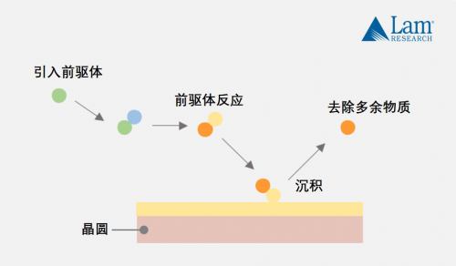
In chemical vapor deposition, the precursor gas will react in the reaction chamber and produce a film attached to the wafer surface and by-products extracted from the chamber.
Plasma enhanced chemical vapor deposition needs the help of plasma to produce reaction gas. This method reduces the reaction temperature, so it is very suitable for temperature sensitive structures. The use of plasma can also reduce the number of deposition, which can often lead to higher quality films.
② Atomic layer deposition
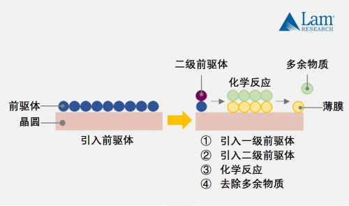
Atomic layer deposition forms a thin film by depositing only a few atomic layers at a time. The key of this method is to cycle the independent steps in a certain order and maintain good control. Coating the precursor on the wafer surface is the first step, and then different gases are introduced to react with the precursor to form the required substances on the wafer surface.
③ Physical vapor deposition
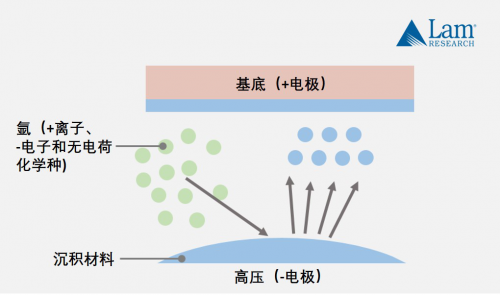
As the name suggests, physical vapor deposition refers to the formation of thin films by physical means. Sputtering is a physical vapor deposition method. Its principle is to sputter the atoms of the target through the bombardment of argon plasma and deposit them on the wafer surface to form a thin film.
In some cases, the deposited film can be treated by ultraviolet heat treatment (UVTP) and other technologies to improve its performance.
The deposition equipment of Fanlin group has excellent accuracy, performance and flexibility, including Altus suitable for tungsten metallization process ® Sola series with post film deposition processing capability ® Series, high density plasma chemical vapor deposition speed ® Strike series, using advanced ALD Technology ® Series and vector ® PECVD series, etc.

